
Editorial Team


Bridgit Mendler’s Northwood Space is pioneering mass-produced ground stations, enabling scalable, high-speed connectivity for the new era of satellite networks and megaconstellations.

SpaceX aims to nearly double launches from Vandenberg in 2025, facing support from federal agencies but strong objections from the state and local communities.

Traditional Medicare will pilot AI-assisted prior authorization in 2026 across six states, focusing on high-risk outpatient services. Clinicians retain final say, but incentives and access concerns loom as CMS tests fraud reduction and “gold card” exemptions. Here’s what providers and patients should know.

OpenArt’s new “one-click story” compresses scripting, visuals, and edits into ready-to-post short videos—fueling viral growth and a fresh IP debate. We break down how it works, adoption signals, what’s next (multi-character, mobile), and practical guardrails creators and brands should follow to stay original and compliant.

OpenAI’s o3 swept the Kaggle AI chess tournament, defeating xAI’s Grok 4–0. The victory fueled the intense rivalry between Altman and Musk, reshaping AI benchmarks.
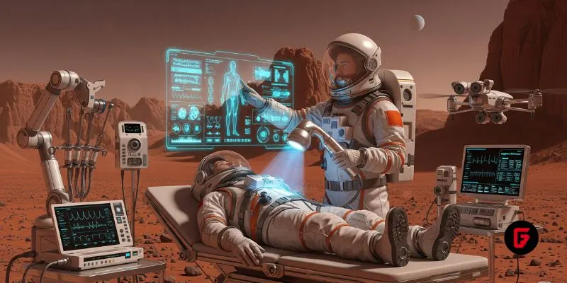
NASA and Google’s AI-powered Crew Medical Officer Digital Assistant enables autonomous diagnoses for astronauts on Mars missions, redefining remote healthcare for space and Earth.

Pinterest’s CEO confirms that fully agentic AI shopping is years away, as the platform invests in AI-powered tools to enhance discovery, inspiration, and personalized shopping experiences for millions.

Shopify’s new AI shopping tools are transforming e-commerce, letting agents and chatbots deliver smooth, personalized shopping and checkout experiences across platforms. Learn how these innovations reshape online retail.

Meta has acquired WaveForms AI, a startup pioneering emotion-detecting voice technology. Learn what this means for Meta’s AI voice ambitions and the future of AI audio.

Tracelight is revolutionizing financial modelling for finance professionals with AI-powered Excel tools that automate complex tasks, reduce errors, and unlock new analysis capabilities. Learn how this next-gen solution changes the future of spreadsheets.
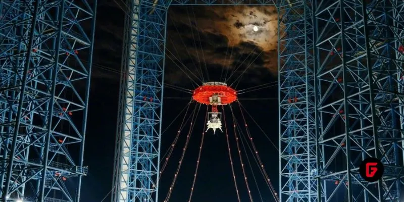
China’s Lanyue lander completed its first major test, showcasing advanced engineering for safe, crewed moon landings before 2030. Explore how this milestone shapes the space race.
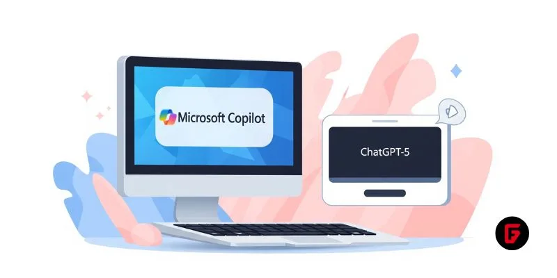
Microsoft rolls out GPT-5 across its Copilot suite, integrating smarter AI for enterprise and personal users. Discover new features, free access, and what sets this launch apart.